Description
Features
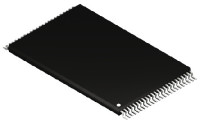
- HIGH DENSITY NAND FLASH MEMORIE
-Cost effective solutions for mass storage applications - NAND INTERFACE
-x8 or x16 bus width.
-Multiplexed Address/ Data
-Pinout compatibility for all densities - SUPPLY VOLTAGE
-3.3V device: VCC = 2.7 to 3.6V : HY27USXX561A
-1.8V device: VCC = 1.7 to 1.95V : HY27SSXX561A - Memory Cell Array
-(512+16) Bytes x 32 Pages x 2,048 Blocks
-(256+8) Words x 32 pages x 2,048 Blocks - PAGE SIZE
-x8 device:(512 + 16 spare) Bytes: HY27(U/S)S08561A
-x16 device: (256 + 8 spare) Words: HY27(U/S)S16561A - BLOCK SIZE
-x8 device:(16K + 512 spare) Bytes
-x16 device: (8K + 256 spare) Words - PAGE READ / PROGRA
-Random access: 3.3V: 12us (max.)1.8V: 15us (max.)
-Sequential access: 3.3V: 50ns (min.) 1.8V: 60ns (min.
-Page program time: 200us (typ.)




Reviews
There are no reviews yet.